Coaxing Hexagonal Silicon-Germanium (SiGe) to emit light for laser action
1. Why we need a silicon laser in the first place?
Every time you stream a video, send an email, browse the internet or read this blog post, your data is for part of its journey, travelling as pulses of light through optical fibres. The lasers that generate this light are not made of silicon. They are built from III-V semiconductor compounds such as indium phosphide or gallium arsenide — materials that emit light efficiently but are expensive to grow, difficult to scale, and fundamentally different from the silicon that powers nearly every electronic chip on the planet.
This creates an undesired divide. The chips that process our data are silicon. The lasers that transmit the data are not. Today, the two are stitched together: a separate III-V laser chip is grown elsewhere and then bonded onto a silicon photonic circuit. It works, but it is costly, hard to scale, and adds an extra manufacturing step that the silicon industry, built on decades of seamless, wafer-scale fabrication, was never designed around.
A laser made directly from a silicon-compatible material would change that. It could be grown and processed in the same factories, on the same wafers, using the same techniques already used to make computer chips. Light sources could become as cheap and as densely packed as transistors are today, paving the way for chips that compute and communicate using the same platform, the same fabrication line, and a fraction of the cost. This is the long-standing goal behind silicon photonics, and it is the question that sits behind my own PhD research.
2. Why does SiGe usually not emit light efficiently?
Conventional silicon and germanium normally crystallise in a cubic structure, the same diamond-like lattice you would find in a silicon wafer. In this form, both elements are indirect band gap semiconductors [1-2]. Silicon dominates electronics yet is almost never used to make light.
In a semiconductor, light is emitted when an electron drops from the conduction band into the valence band and recombines with a hole. For this to happen efficiently, the electron also needs to conserve momentum, not just energy. In direct band gap materials, the conduction band minimum and valence band maximum sit at the same point in momentum space, so the transition happens easily and a photon is emitted, as shown in Figure 1. In indirect materials like cubic silicon and germanium, the two band extrema sit at different momenta. The transition can still happen, but only with the help of a lattice vibration, a phonon, to carry away the extra momentum. This makes radiative recombination slow and inefficient. Most of the energy is instead lost as heat, dissipated through vibrations in the crystal lattice rather than released as light (poor light emission). This is the central reason silicon-based materials, despite ruling the electronics industry, have historically been unsuitable for lasers or efficient light-emitting devices.
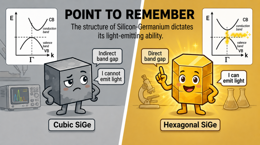
Figure 1. Schematics of cubic SiGe (indirect band gap) with no light emission while hexagonal SiGe (direct band gap) emits light efficiently — state-of-the-art.
Interestingly, the story changes when SiGe is grown not in its usual cubic form, but in a hexagonal crystal phase. In this alternative crystal structure, the electronic band structure shifts, and for certain germanium-rich compositions, the band gap turns from indirect to direct. Electrons can then recombine with holes far more efficiently, without needing a phonon to help conserve momentum. The result is genuinely efficient light emission, from a material that is chemically almost identical to the silicon that is already used in every electronic device.
This single structural twist is what has reopened the question of silicon-compatible lasers after decades of researchers assuming it was simply off the table.
3. Towards silicon-based lasers
My research focuses on understanding the optical properties of hexagonal SiGe nanowires and how their crystal structure, composition, strain and doping influence the way they emit light. Nanowires provide an ideal platform for growing and stabilising the hexagonal crystal phase of SiGe, allowing us to investigate its unique optical properties.
At present, hexagonal SiGe are mainly grown by using a hexagonal Gallium Arsenide (GaAs) nanowire as a template in the form of core shell nanowires, as shown in Figure 2. Since SiGe naturally crystallises in its conventional cubic crystal structure, a hexagonal GaAs nanowire is currently used as a template to guide the growth of the SiGe shell into the desired hexagonal phase. This approach enables researchers to investigate the intrinsic optical properties of hexagonal SiGe. In the long term, however, new epitaxial growth methods will need to be developed in order to produce hexagonal SiGe without III-V semiconductor templates, paving the way for a fully monolithic, standard chip-compatible group-IV photonics platform.
The light emission from hexagonal SiGe/hex-Ge has already been demonstrated [3-4], but the dream of practical lasing has not yet been achieved. By carefully engineering these nanowires and exploring structural modulation, we hope to move closer to efficient silicon-compatible light sources and eventually, nanoscale lasers. The light emission from hexagonal SiGe has already been demonstrated [3]. One of the strengths of this project is the collaboration between the Institut des Nanotechnologies de Lyon (INL) and RMIT University. INL is equipped with a unique molecular beam epitaxy (MBE) system capable of growing high-quality III-V/group-IV semiconductor nanowires [4] while RMIT brings complementary expertise in fabricating and characterising optoelectronic devices. Together, these capabilities provide a favourable environment for advancing silicon-compatible photonic technologies.
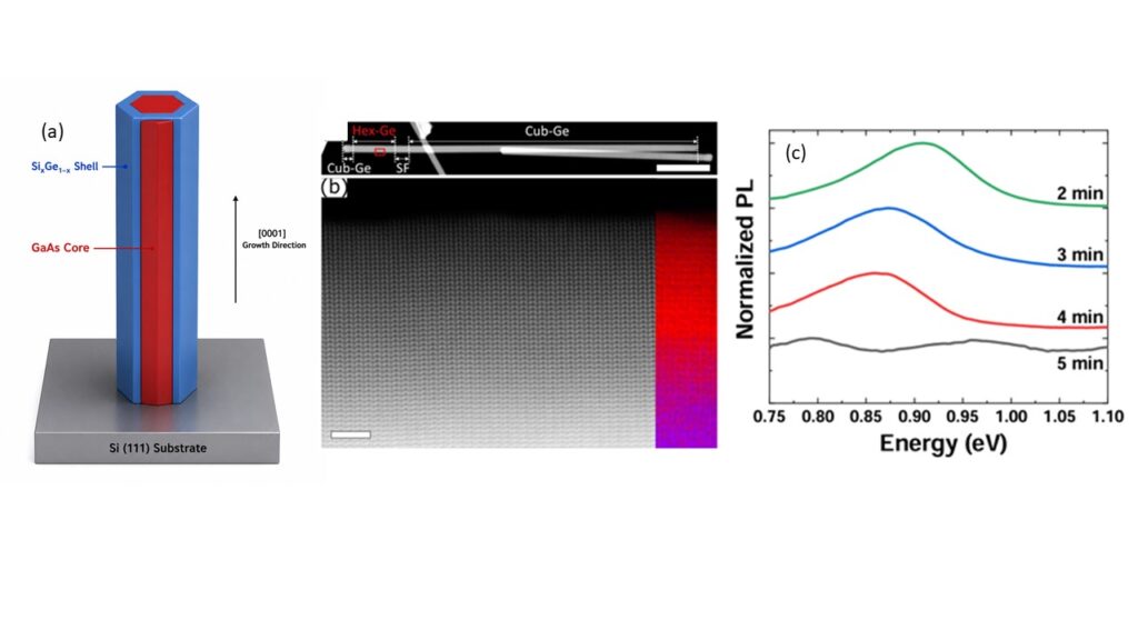
Figure 2. (a) Schematic of core shell Nanowires of Hex- GaAs/SiGe. (b) A highly magnified electron microscope image of a NW. Scale bar is 500 nm. A highly magnified electron microscope image of (b) the WZ structure with a superimposed Ga (blue) and Ge (red) maps extracted from multiple linear least square fitting (c) low temperature photoluminescence spectra of Hex-GaAs/Ge/GaAs [4].
The prize at the end of this is the possibility of integrating optical communication directly onto silicon chips. Modern electronics rely on electrons to process information, while optical systems use photons to move it at high speed over long distances with very little loss. Bringing both onto the same platform, the same material, the same fabrication process, could lead to devices that are faster, more energy-efficient and far simpler to manufacture than the hybrid systems we rely on today [4].
There is still a long way to go before hexagonal SiGe nanowires become practical laser materials. But that distance is exactly what makes this work worth doing. Sometimes scientific progress starts by persuading a material to behave in a way nature did not originally intend and seeing what becomes possible once it does.
References
- Oliphant, E., et al., Why does silicon have an indirect band gap? Materials Horizons, 2025. 12(9): p. 3073-3083.
- Santos-Castro, G., et al., Silicon and germanium adamantane and diamantane monolayers as two-dimensional anisotropic direct-gap semiconductors. Physical Review B, 2023. 108(3): p. 035302.
- Fadaly, E.M., et al., Direct-bandgap emission from hexagonal Ge and SiGe alloys. Nature, 2020. 580(7802): p. 205-209.
- Dudko, I., Hexagonal Ge on self-assisted GaAs Nanowires by Molecular Beam Epitaxy. 2025, Ecole Centrale de Lyon; RMIT University (Melbourne).
Find out more about my research project here.